Silicon Photonics: The Next Silicon Revolution?
Bringing the enormous scale of CMOS manufacturing to the world of light has been a goal for decades. Asianometry traces silicon photonics from a 1987 paper to today's data-center transceivers — and asks whether there's a market big enough to make it matter.
Watch on YouTubeThe short version
- Silicon photonics moves data with light instead of electrons, hoping to bring CMOS economics to optics — but pure silicon can neither emit light nor natively modulate it.
- Two material problems define the field: silicon's indirect band gap means it can't lase, and its lack of the Pockels effect means it can't modulate. The workarounds are external or bonded lasers and engineered modulators.
- The field really starts with Richard Soref's 1987 paper "Electrooptical Effects in Silicon." Intel set the milestones — a high-speed modulator in 2004 (Mach-Zehnder) and a fully integrated CMOS transceiver in 2012 (ring modulator, 90nm).
- The first real market is the data center, where integrated transceivers replace plug-in optics. LiDAR is a promising second.
- The catch is volume — the entire transceiver industry needs only ~40-60k wafers a year. For a megafab like TSMC that's barely a month's output, which is why TSMC is betting on packaging instead, and why this may stall like MEMS did.
01 · Deep tech
A magic silicon technology
Silicon photonics is what you get when you apply modern nanoscale CMOS processes to optics — the same move that turned mechanical structures into MEMS, pointed now at light. Instead of pushing electrons through copper, you transmit and steer photons on a chip.
If MEMS is the result of applying modern nanoscale CMOS processes to the mechanical world, then doing the same for the optical realm gives us silicon photonics.— Asianometry
02 · The five ingredients
What a photonic system needs
The 1970s dream was a monolithic chip — built from one material system — that could generate, route, and read light. Asianometry splits it into five parts: a light source (usually a laser), passive structures to bend and split the light, a modulator and a photodetector to convert between electrical and optical signals, and ordinary CMOS electronics to run the whole thing.
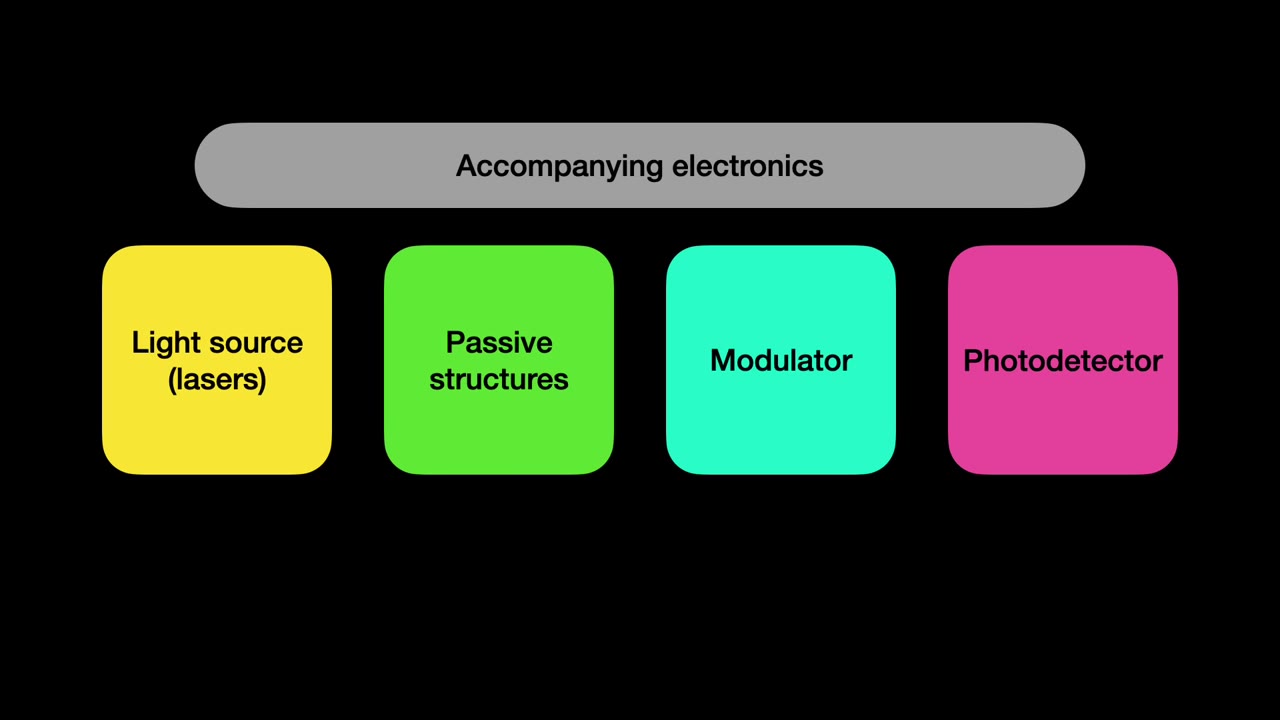
Light source
A laser to produce the light, ideally on-chip.
Passive structures
Waveguides that bend, guide, filter, split, and combine — optical fiber's job, but on the die.
Modulator + photodetector
Convert electrical signals to light and back; a part that does both is a transceiver.
CMOS electronics
Traditional support logic for encoding and decoding.
03 · The two issues
Where silicon comes up short
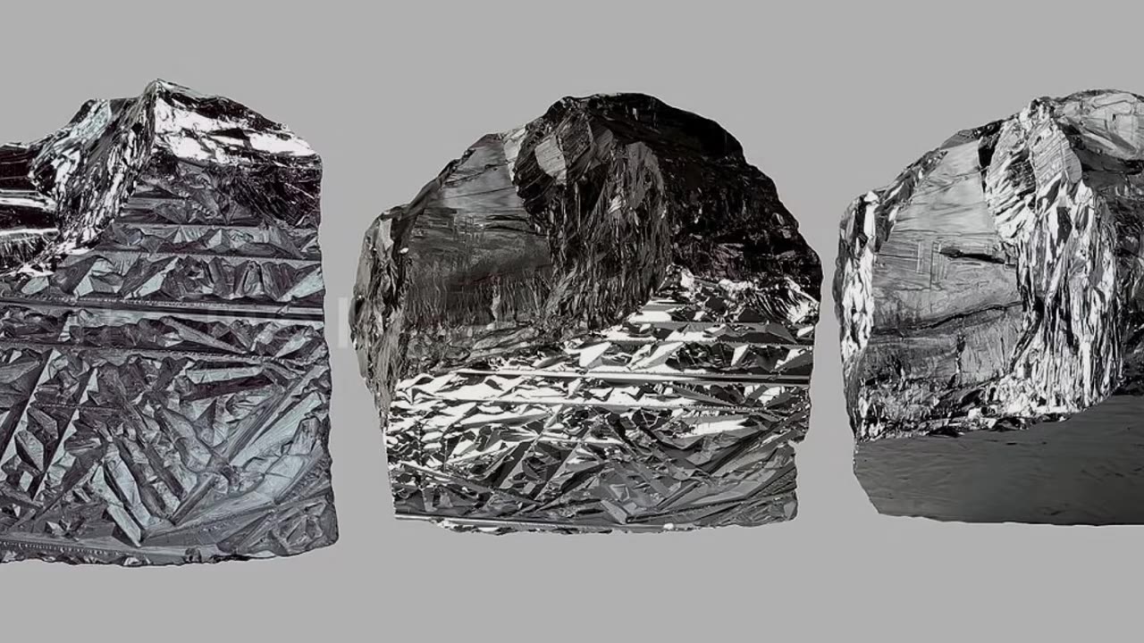
Two properties of crystalline silicon make a fully integrated, all-silicon photonic chip very hard. First, silicon has an indirect band gap, so on its own it can't emit light — no LED, no laser, no source. Second, silicon doesn't show the Pockels effect, the property that lets an electric field change a material's refractive index — so it can't natively modulate light either.
04 · The real beginning
Soref and the workarounds
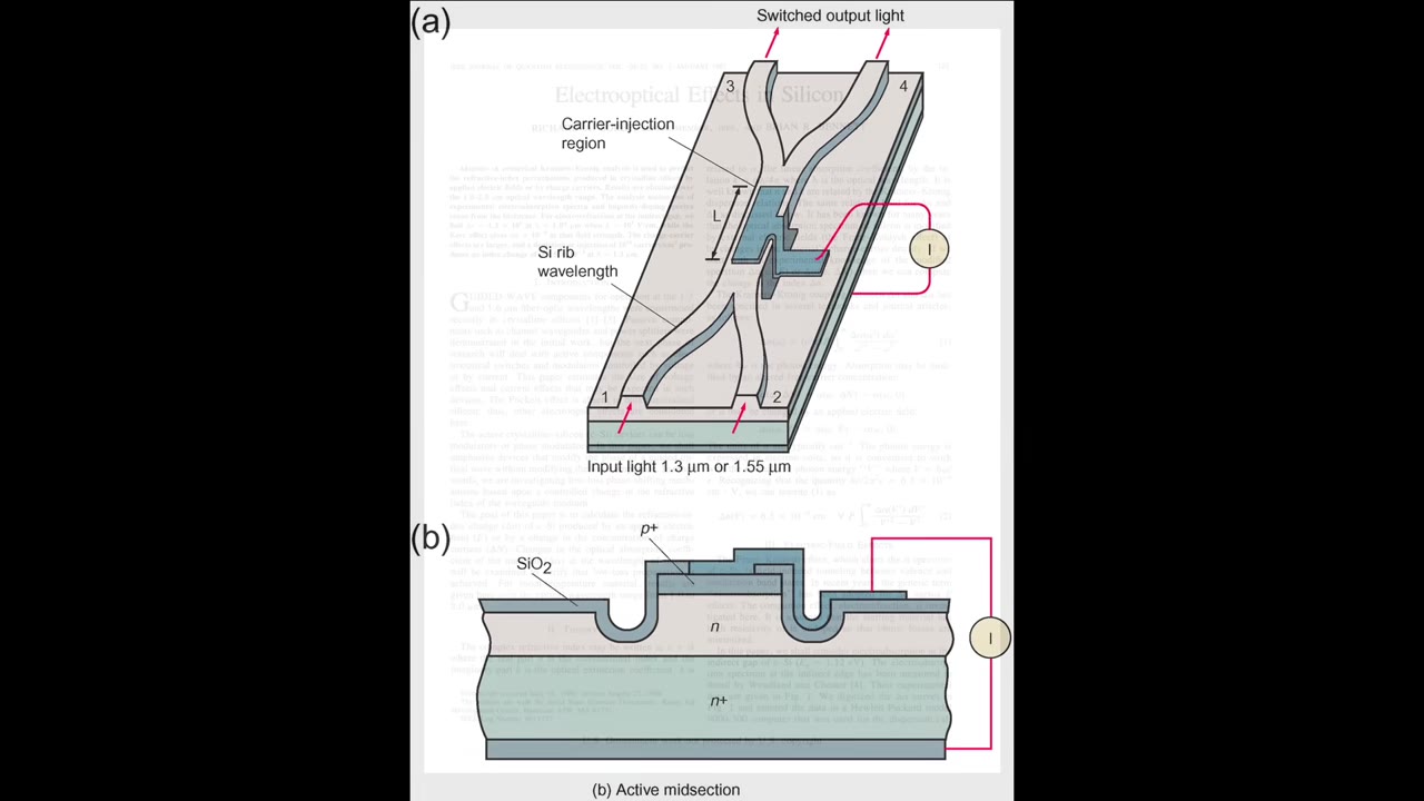
Silicon photonics as we know it begins in the mid-1980s with Richard Soref. His 1987 paper, "Electrooptical Effects in Silicon," showed silicon could be manipulated to adjust its refractive index, and the industry soon built a semiconductor's basic p-n junction inside a photonic waveguide. For the missing laser, engineers settled for workarounds: an external laser sitting off-chip, or bonding a pre-made laser made of another material — indium phosphide — onto the silicon, which is called hybrid integration.
A silicon-based laser is considered the holy grail of the silicon photonics space, the final piece of the puzzle.— Asianometry
05 · The modulator milestones
Intel's breakthroughs
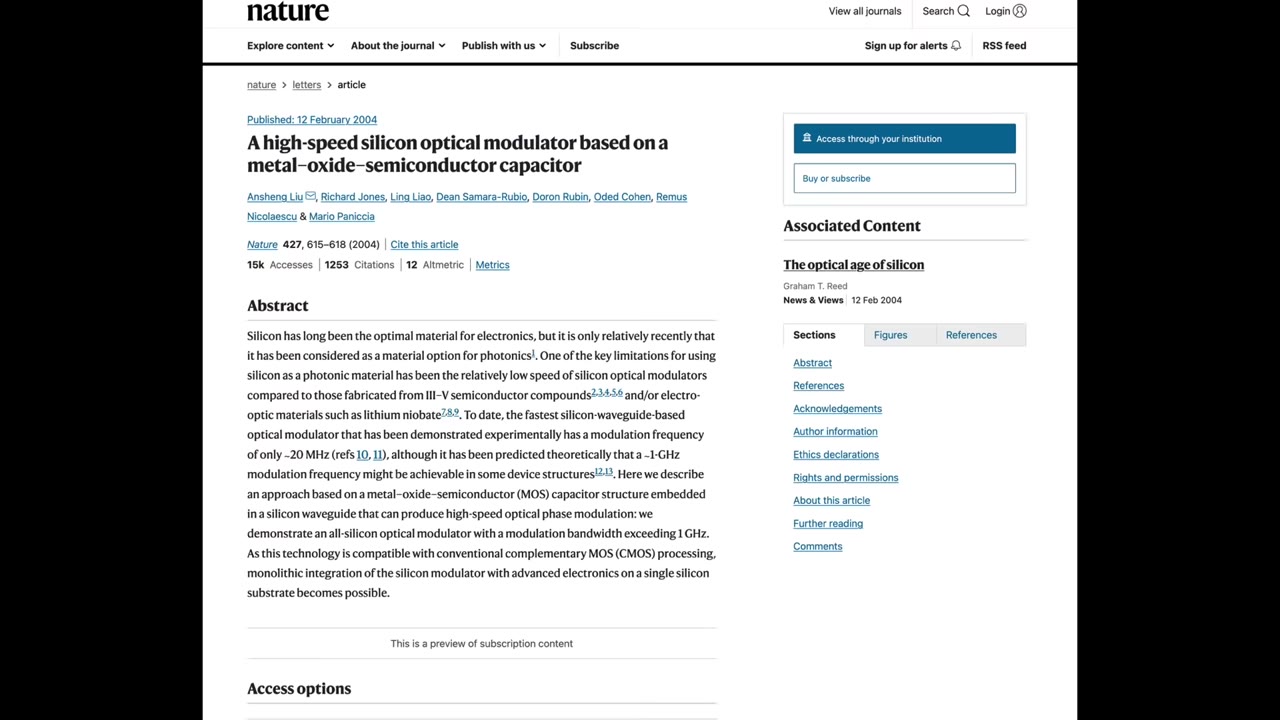
With the light source handed off to a workaround, the modulator became the proving ground. In 2004 Intel announced the first silicon-based high-speed optical modulator — over 1 GHz of bandwidth — using a Mach-Zehnder interferometer (MZI), which splits light into two paths and recombines them to encode 1s and 0s. In 2012 Intel followed with its first fully integrated CMOS silicon photonics transceiver: four channels at 25 Gbit/s each, on a 90nm process, using a smaller ring modulator instead of the MZI.
- 2004 — first high-speed modulatorMach-Zehnder design, over 1 GHz of bandwidth, heavy press attention.
- 2012 — first integrated transceiverFour channels at 25 Gbit/s, 90nm CMOS, compact ring modulator.
06 · First market
Transceivers in the data center
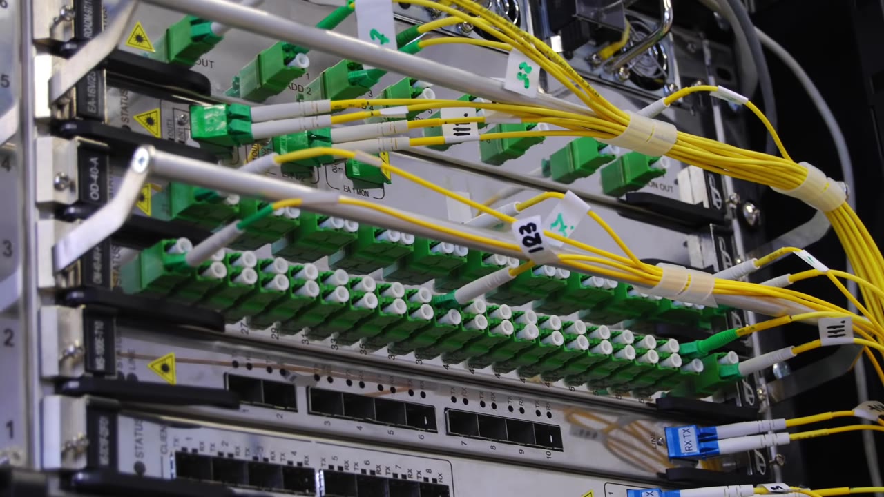
The first big commercial opening is inside the hyperscaler data center — Alibaba, AWS, Google, Microsoft — where more data moves between a few hundred servers in one building than crosses between the east and west halves of the US public internet. Transceivers normally plug into the switch at the top of each rack; silicon photonics integrates that function onto the chip itself, saving cost, power, and labor while clearing a bandwidth bottleneck. Intel, Cisco, and MACOM already sell millions of units a year.
There is more data transmitting between a couple hundred servers within a single hyperscaler data center than what goes between the east and west halves of the United States public internet.— Asianometry
07 · Second market
LiDAR and sensors
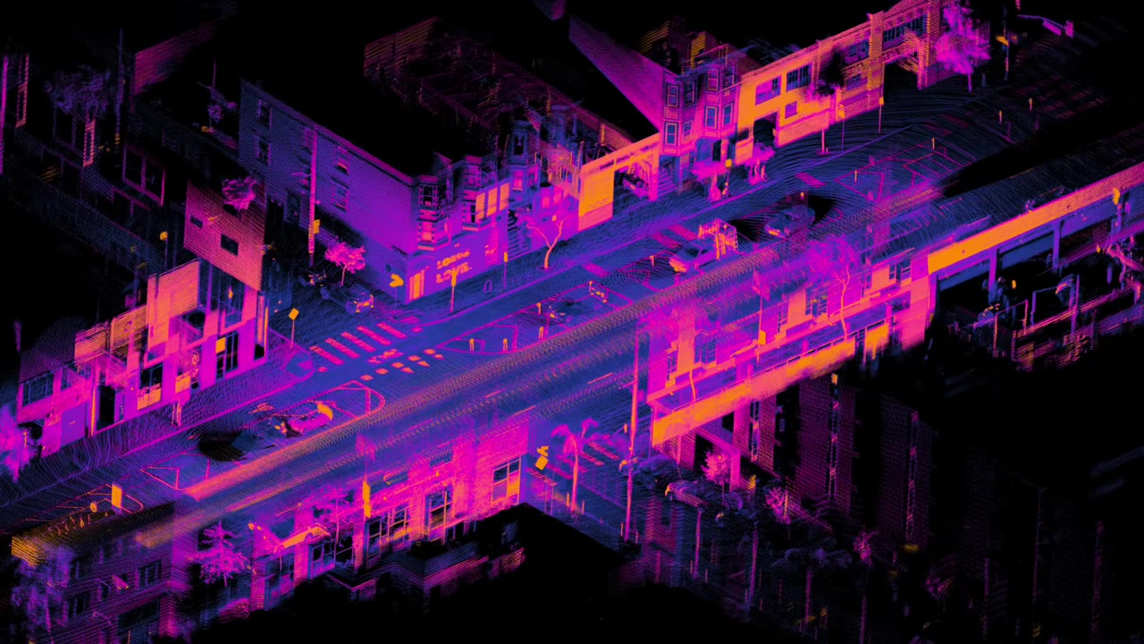
Past the data center, the most promising market is LiDAR — using light instead of radio waves to build a 3D picture of a scene, with finer resolution than radar and a central role in self-driving. The problem is cost and bulk: one system can run up to $70,000. Putting the discrete optical parts onto a single silicon photonics chip could cut both. Intel subsidiary Mobileye has shown a LiDAR system-on-chip with integrated lasers, in a crowded field that also includes PointCloud, Aeva, Voyant Photonics, and Analog Photonics.
08 · The supply side
SOI wafers and the foundries
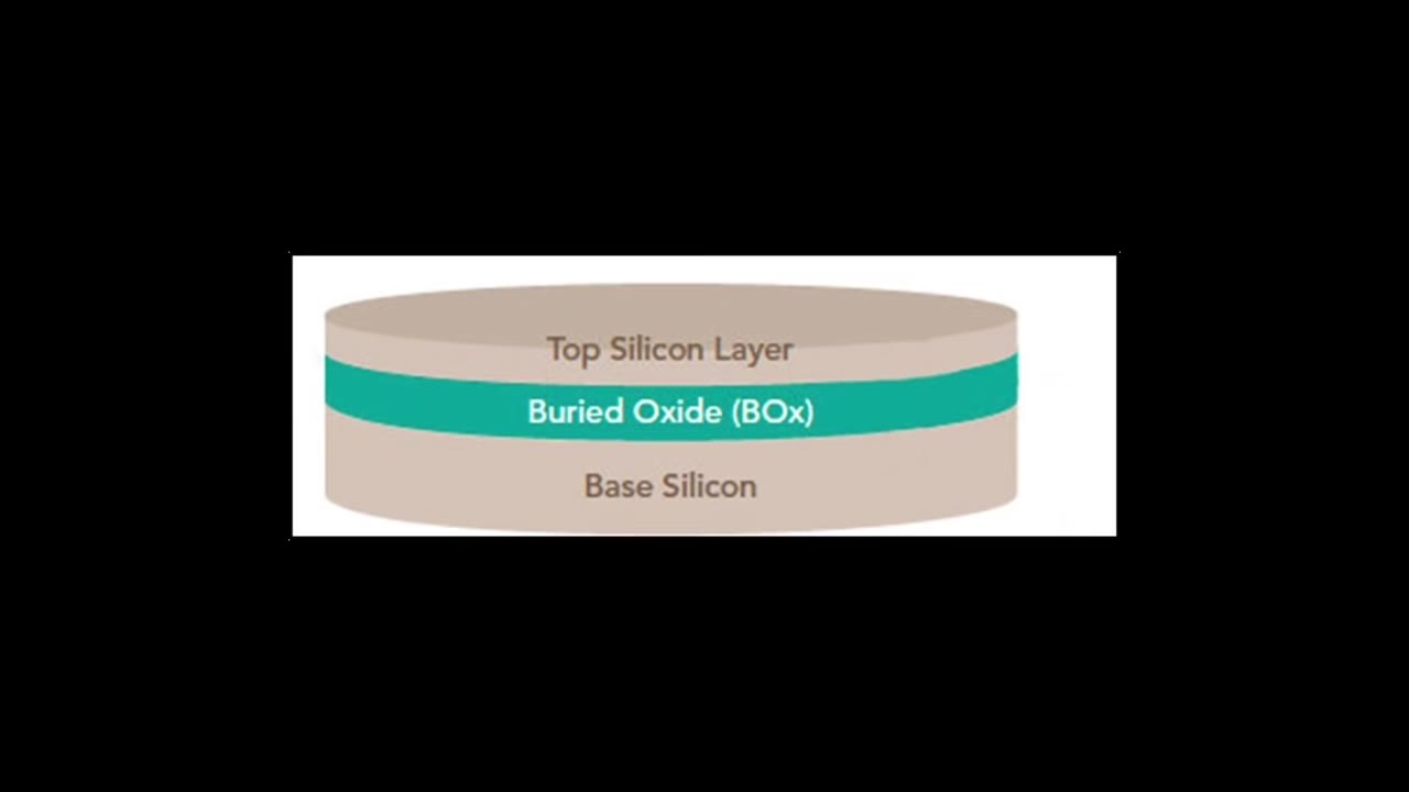
Silicon photonics is built on silicon-on-insulator (SOI) wafers — a top silicon layer over a buried oxide over base silicon — where the layers' contrasting refractive indices help confine the light. That makes it a specialty node a couple of years behind the leading edge, which suits foundries that aren't chasing 3nm. GlobalFoundries leads, partly on IP it gained acquiring IBM's microelectronics division in 2014 (per Dylan Patel of SemiAnalysis). Intel has long been an R&D pioneer, while TSMC has stayed light on it, focusing instead on packaging that lets photonic chiplets sit beside traditional chips.
09 · The catch
A market big enough?
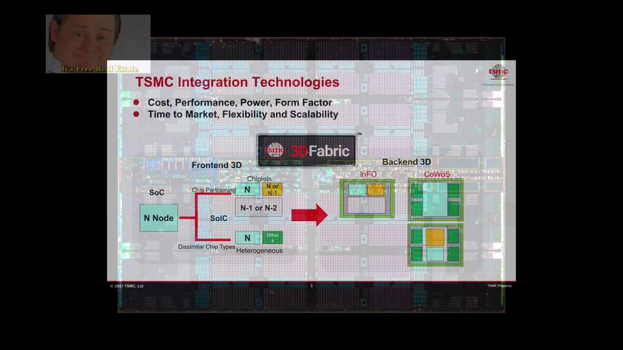
Here's the bind. Photonic components can't be smaller than the wavelength of the light they carry — about 1 micrometer — while electrons have wavelengths of a few nanometers; at a 7nm node, that one square micrometer could hold over 100 transistors. So the economics push away from dense monolithic photonics and toward packaging photonic chiplets next to ordinary silicon — which is exactly what TSMC seems to be doing. And the volume is small: the entire transceiver industry needs only ~40-60k wafers a year, less than a month at a single megafab. The risk is that silicon photonics ends up like MEMS — a genuine unit-volume success whose value all flows to packaging, stopping short of becoming the next silicon revolution.